发布时间:2012-05-2 阅读量:1720 来源: 我爱方案网 作者:
【导读】在能源挑战日趋严峻的背景之下,太阳能成为了一种新型和快速壮大的技术。以廉价和高效的方式发电是关键的需求,而 PXS20 是32位双核双发射的Power Architecture微控制器,拥有可满足上述两项需求的强大特性,从而使其成为太阳能逆变器设计的必然方案。想了解PXS20如何在逆变器中发挥作用,请看本文报道...
Freescale公司的PXS20是32位双核双发射的Power Architecture微控制器,满足安全标准IEC61511和IEC61508 (SIL3),能降低设计复杂性和减少所用元件。PXS20采用高性能的e200z4d双核,核频率高达120MHz,双发射级流水线核,可变长度编码(VLE),集成了存储器管理单元(MMU)和信号处理引擎,带误差检测代码的4KB指令缓存,主要用在消费类电子,工业控制,太阳能逆变器,机器人和马达控制等。本文介绍了PXS20主要特性,方框图,以及采用PXS20控制的太阳能三相逆变器基本架构,1kW,3kW,10kW和大于10kW以及微逆变器的太阳能三相逆变器解决方案架构图。
The PXS20 series microcontrollers are system-on-chip devices that are built on Power Architecture technology and contain enhancements that improve the architecture’s fit in embedded applications, include additional instruction support for digital signal processing (DSP) and integrate technologies such as an enhanced time processor unit, enhanced queued analog-to-digital converter, Controller Area Network, and an enhanced modular input-output system.
The PXS20 family of 32-bit microcontrollers is the latest achievement in integrated safety controllers. The advanced and cost-efficient host processor core of the PXS20 family complies with the Power Architecture embedded category. It operates at speeds as high as 120 MHz and offers high-performance processing optimized for low power consumption. It capitalizes on the available development infrastructure of current Power Architecture devices and is supported with software drivers, operating systems and configuration code to assist with users’ implementations.
.jpg)
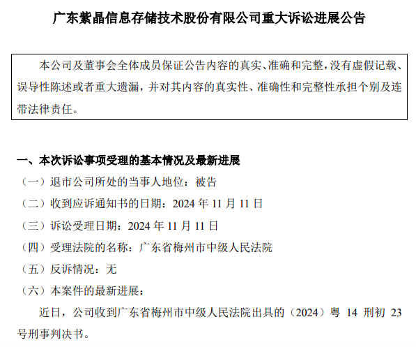
采用PXS20控制的太阳能三相逆变器
Today, the demand for green energy is very strong. One possible option for meeting this demand is to convert solar energy into electrical energy. This process is supported by the photovoltaic (PV) solar panel, which produces various DC output voltages and output power.
In the conversion from DC to AC power, dedicated inverters maintain the right working point for the solar panel to maximize its use of solar energy. Freescale Semiconductor’s processors built on Power Architecture® technology are well suited for the control of such inverters. Freescale offers a broad portfolio of PX microcontrollers built on Power Architecture technology for power management and motor control applications. The target portfolio for these devices includes consumer, industrial, and other markets. One microcontroller from the PX Series of Power Architecture devices can control the whole 3-phase inverter in various configurations and output power.
.jpg)
.jpg)
.jpg)
.jpg)
.jpg)
.jpg)
.jpg)
PXS20主要特性:
紫晶存储犯欺诈发行证券罪,判处罚金人民币3700万元;公司实际控制人郑穆、罗铁威及原财务总监李燕霞等10名核心管理人员,全部被判处有期徒刑,刑期最高达七年六个月。

近日,日产汽车和总部位于英国的自动驾驶初创公司Wayve签署协议,合作开发基于人工智能的驾驶辅助系统。

京东开启招聘存算一体芯片设计工程师计划,薪酬高达“40K-100K*20薪”

日本芯片制造商铠侠(Kioxia)计划于2026年在其岩手县晶圆厂开始生产新一代NAND闪存芯片。

一系列诉讼指控芯片制造商英特尔、AMD及德州仪器公司,未能有效阻止其技术被用于俄罗斯制造的武器。


