发布时间:2012-06-26 阅读量:1306 来源: 我爱方案网 作者:
Supertex公司的HV7355是八路单极高压高速超声波脉冲发生器,输出电压0V-150V,源和沉电流为±1.5A,连续波模式±300mA,高达18MHz工作频率,2.5V-3.3V CMOS逻辑接口,主要用在手提超声波图像仪,压电传感器驱动器,NDT超声波发送器和脉冲波形发生器.本文介绍了HV7355主要特性, 典型应用电路以及150V/1.5A单极超声波脉冲器演示板HV7355DB1主要特性, 方框图和电路图.
Eight Channel, High Speed, Unipolar, Ultrasound Pulser 1.5A 150V
The Supertex HV7355 is an eight-channel, unipolar, high voltage, high-speed pulse generator. It is designed for medical ultrasound applications. This high voltage and high speed integrated circuit can also be used for other piezoelectric, capacitive or MEMS sensors in ultrasonic nondestructive detection and sonar ranger applications.
The HV7355 consists of a controller logic interface circuit, level translators, MOSFET gate drivers and high current P-channel and N-channel MOSFETs as the output stage for each channel.
The output stages of each channel are designed to provide peak output currents over ±1.5A for pulsing, when MC = 1, with up to 150V swings. When MC = 0, all the output stages drop the peak current to ±500mA for low-voltage CW mode operation to save power. This direct coupling topology of the gate driver not only saves one high voltage capacitor per channel, but also makes the PCB layout easier.
HV7355主要特性:
►► HVCMOS technology for high performance
►► High density integrated ultrasound transmitter
►► 0 to +150V output voltage
►► ±1.5A source and sink current (min.)
►► ±300mA current in CW mode
►► Up to 18MHz operating frequency
►► Matched delay times
►► Built-in gate driver floating voltage regulator
►► 2.5 to 3.3V CMOS logic interface
HV7355应用:
►► Portable medical ultrasound imaging
►► Piezoelectric transducer drivers
►► NDT ultrasound transmission
►► Pulse waveform generator
.gif)
图1.HV7355典型应用电路
150V/1.5A单极超声波脉冲器演示板HV7355DB1
150V, 1.5A, Unipolar Ultrasound Pulser Demoboard
The HV7355 is a monolithic eight-channel, high-speed,high voltage, unipolar ultrasound transmitter pulser. This integrated, high performance circuit is in a single, 8x8x0.9mm, 56-lead QFN package.
The HV7355 can deliver guaranteed ±1.5A source and sink current to a capacitive transducer with 0 to +150V peak voltage. It is designed for medical ultrasound imaging and ultrasound material NDT applications. It can also be used as a high voltage driver for other piezoelectric or capacitive MEMS transducers, or for ATE systems and pulse signal generators as a signal source.
The HV7355’s circuitry consists of controller logic circuits, level translators, gate driving buffers and a high current and high voltage MOSFET output stage. The output stages of each channel are designed to provide peak output currents typically over ±1.5A for pulsing, with up to 150V swings. The upper limit frequency of the pulser waveform is dependent upon the load capacitance. With different capacitance load conditions the maximum output frequency is about 20MHz.
This demoboard datasheet describes how to use the HV7355DB1 to generate the basic high voltage pulse waveform as an ultrasound transmitting pulser.
The HV7355 circuit uses DC-coupling from a 3.3V logic input to output TX0~7 internally, therefore the chip needs three sets of voltage supply rails: VLL (+3.3V), VDD/VSS (+/-5.0V) and VPP (up to +150V). The VPP high voltage supply can be changed rather quickly, compared to the capacitor gatecoupled driving pulsers. This direct coupling topology of the gate drivers not only saves two high voltage capacitors per channel, but also makes the PCB layout easier.
The control signal logic-high voltage should be the same as the VLL voltage of the IC, and the logic-low should be referenced to GND.
The HV7355DB1 output waveforms can be displayed using an oscilloscope by connecting the scope probe to the test points TX0~7 and GND. The soldering jumper can select whether or not to connect the on-board dummy load, a 330pF capacitor paralleling with a 2.5kΩ resistor. The test points can be used to connect the user’s transducer to easily evaluate the pulser.
.gif)
图2.演示板HV7355DB1方框图
.gif)
图3.演示板HV7355DB1电路图
.gif)
图4.演示板HV7355DB1外形图
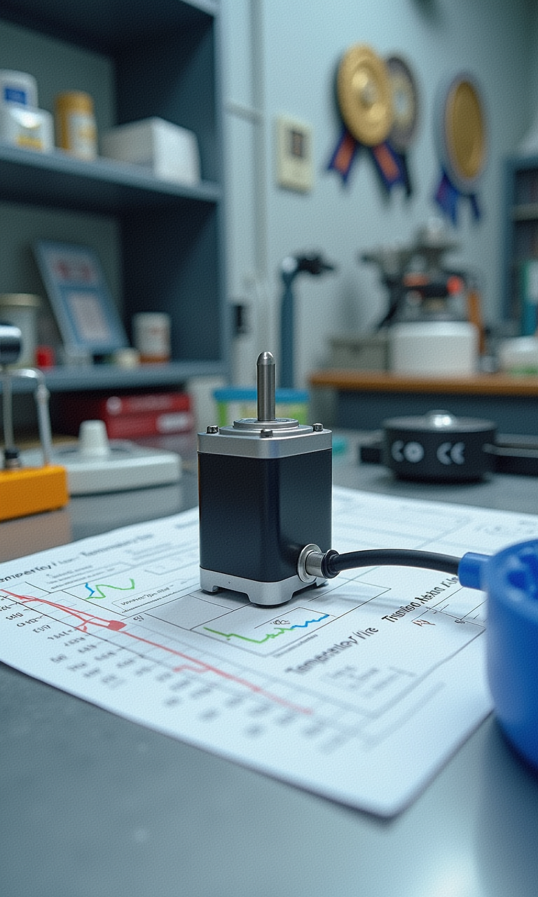
BLDC电机技术演进正朝着更高性能、更智能化、更集成化和可持续的方向快速发展
BLDC电机凭借其皆能、静音和智能化控制方面的优势广泛应用于各类家电产品中

本文将系统性地剖析BLDC无刷电机的技术原理、核心优势,并深入探讨其在关键行业中的应用场景与未来发展趋势
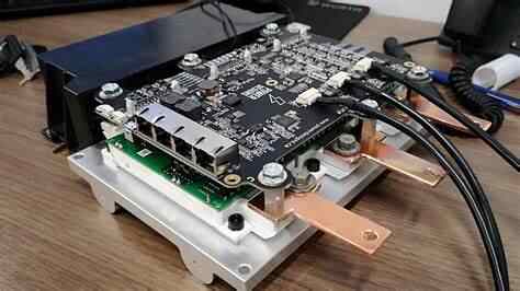
高精度运动控制领域对MCU的要求极为严苛:需要高性能内核、高精度定时器/PWM、高速高分辨率ADC、丰富的通信接口以及强大的实时处理能力
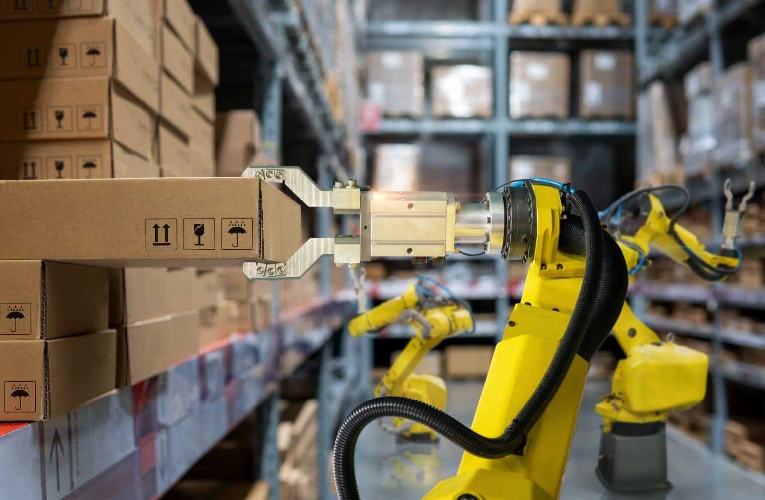
国产高性能MCU在机器人技术中的应用已远不止关节控制,其凭借高集成度、低功耗、强实时性及不断攀升的算力,正全面渗透至机器人系统关键场景


